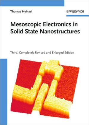
Mesoscopic Electronics in Solid State Nanostructures
This updated and expanded third edition of this successful work includes a new, comprehensive introduction to the recursive Green's function technique applied to model solid state nanostructures.\ From the contents:\ * An Update of Solid State Physics\ * Surfaces, Interfaces, and Layered Devices\ * Experimental Techniques\ * Important Quantities in Mesoscopic Transport\ * Magnetotransport Properties of Quantum Films\ * Quantum Wires and Quantum Point Contacts\ * Theory of Ballistic...
Search in google:
This updated and expanded third edition of this successful work includes a new, comprehensive introduction to the recursive Green's function technique applied to model solid state nanostructures. Focusing on the physical background as well as on technical details of the technology, this is a must-have book for beginners in the field.
\ Mesoscopic Electronics in Solid State Nanostructures\ \ \ \ By Thomas Heinzel\ \ \ John Wiley & Sons\ \ \ \ Copyright © 2003\ \ Thomas Heinzel\ All right reserved.\ \ \ ISBN: 3-527-40375-2\ \ \ \ Chapter One\ \ \ An Update of Solid State Physics\ \ Mesoscopic systems are fabricated from various bulk materials, which are often, but not always,\ semiconductors. Some basic knowledge of their bulk properties is important and represents\ the major part of this chapter. Although this is in many respects just a polishing up\ of solid state physics at an introductory level, we introduce many specifics of the materials of\ interest along the way, in particular of Si and GaAs. Occasionally, conventional metals and\ carbon crystals are mentioned as well, although the reader is supposed to know their basics.\ We begin by a brief recapitulation of the most relevant crystal structures in section 2.1,\ and proceed by looking at the corresponding electronic band structures of the materials in\ section 2.2. Here, it is of particular importance to model the valence and the conduction\ bands around their maximum and minimum, respectively. As always, we can approximate\ the energy dispersions near the band extremal points by parabolas, which leads to the concept\ of effective masses. We shall see that within this approximation, the crystal properties can\ be "put aside" in many cases. Instead, the chargecarriers behave like free electrons with a\ modified mass. The properties of electrons and holes within the effective mass approximation\ are looked at in section 2.3. Also, the effective mass approximation allows us to work with\ envelope wave functions. With this approach, superpotentials like those frequently met in\ nanostructures, can be treated with a Schrodinger equation for just this superpotential. The\ crystal potential enters only via the effective masses as well as via its dielectric constant.\ This is a very elegant concept, which simplifies our life substantially in subsequent chapters.\ Developing this approximation is the topic of section 2.4.\ Doping is the standard way to fill the bands of a semiconductor with a significant and\ temperature-independent carrier density. The important issues concerning doping are reviewed\ in section 2.5. In the subsequent section, we look at the transport properties of electron\ gases within the simplest version of the Boltzmann model. We will occasionally use\ these results when looking at diffusive samples later on. Furthermore, it is of help to know\ the approximations that enter this model, in order to appreciate the deviations we will look\ at in subsequent chapters. A non-vanishing resistance indicates that some sort of scattering\ mechanism must be present, which are the topic of section 2.7. Finally, we spend a few words\ on screening in section 2.8.\ Readers who discover that parts of this chapter are white spots on their map of solid\ state physics knowledge are encouraged to consult one of several excellent introductory textbooks\ for further information, e.g., [Ashcroft1985, Ziman1995]. If everything sounds familiar,\ please consider this chapter as a warm-up exercise!\ \ 2.1 Crystal structures\ Many elements and compounds crystallize in a face centered cubic (fcc) lattice. This is not\ surprising, since this crystal structure represents one of the two closed packings possible,\ which one might naively expect to occur when identical or very similar spheres are piled up.\ Both Si and GaAs have this lattice structure. The lattice constant a is the length of one edge of\ a unit cell. Si is composed of two fcc lattices shifted relative to each other by (a/4, a/4, a/4). This crystal\ structure is also known as the diamond structure. GaAs also has a two-atom base,\ except that here, the one base atom is Ga, the other one As. This is the zincblend lattice. The\ lattice constants are 0.565 nm for Si and 0.543 nm for GaAs (both numbers hold for room\ temperature). Fig. 2.1 shows the Si and the GaAs structure.\ The reciprocal lattice of an fcc lattice is a body-centered cubic (bcc) lattice. Since the crystal\ momentum is invariant under translations by reciprocal lattice vectors, we can represent the\ behavior of electrons and phonons within one elementary cell of the reciprocal lattice, which\ is always chosen as the first Brillouin zone. For an fcc lattice, this is a truncated octahedron,\ composed of 6 squares and 8 hexagons, see Fig. 2.1. The center of the first Brillouin zone is\ labelled the [GAMMA]-point, while the centers of the hexagons and squares are referred to as L- and\ X-points, respectively. Occasionally, one hits upon more exotic directions of lower symmetry,\ such as K,U, and W, which are located at the center of the edges and at the corners of the first\ Brillouin zone.\ Germanium crystallize in a diamond structure like silicon. This is also the case for many\ compound semiconductors. Any binary combination of Al, Ga, or In with As, Sb or P (the so-called\ III-V compounds) will result in a zincblend lattice. Combining these group III elements\ with nitrogen can lead to both a fcc lattice or a hexagonal lattice, depending on the crystallization\ process and the subsequent treatment. This is also the case for most II-VI compounds,\ such as CdSe or ZnS (which gave the zincblend structure its name, after all). Thus, when\ working with semiconductors, you will barely ever meet any further crystal structures. To\ finish this section, let us have a look at a particular simple lattice, namely a sheet of graphite,\ the second crystal structure carbon forms besides diamond. It consists of a hexagonal, lattice\ of [sp.sup.2] - hybridized carbon atoms (Fig. 2.2).\ \ Question 2.1: Calculate the reciprocal lattice of the graphite sheet and construct its first\ Brillouin zone.\ The reciprocal lattice is again hexagonal. The center of the first Brillouin zone is denoted\ by [GAMMA], the corners by K, and the centers of the edges are labelled L, respectively (Fig. 2.2).\ \ 2.2 Electronic energy bands\ An electronic energy band is an energy interval in which electronic states are allowed in the\ crystal. The bands are separated by band gaps. This energy structure is obtained by solving\ the Schrodinger equation for electrons in the crystal\ (2.1) [MATHEMATICAL EXPRESSION NOT REPRODUCIBLE IN ASCII]\ Here, the electronic wave functions depend on both the wave vector k and the spatial coordinates\ r. They are denoted by [phi](k,r), while [V.sub.crystal](r) is the crystal potential.\ Elementary solid state physics tells us that the wave functions have to obey Bloch's theorem, which states\ that they are of the form\ (2.2) [MATHEMATICAL EXPRESSION NOT REPRODUCIBLE IN ASCII]\ where [u.sub.k](r) has the periodicity of the crystal lattice. Such wave functions are Bloch functions.\ The task is to determine the eigenvalues [epsilon](k) and eigenvectors, which is usually done by transforming\ the differential equation into an algebraic equation. An exact solution, though, is only\ possible for some special cases. Some reasonable approximation is therefore called for. How\ eq. (2.2) is then solved in detail depends on the model. The nearly free electron model starts\ from a free electron gas and treats a weak periodic crystal potential within perturbation theory.\ Here, the band gaps emerge from interferences of the electronic waves that get scattered at the\ crystal potential, which results in standing waves at the edges of the Brillouin zones. The\ reader is referred to the extensive literature on solid state physics for details. Here, we look at\ a different approach, which constructs the electronic eigenstates from those of the individual\ atoms that form the crystal. This approach is known as the tight binding model. Within this\ picture, the energy bands and the band gaps are remainders of the discrete energy spectrum of\ the atoms.\ The tight-binding model is based on the assumption that the atomic orbitals [[xi].sub.j](r) are a\ good starting point for constructing Bloch waves [[xi].sub.j](k,r). Let us assume there is only one\ atom per unit cell. We can obtain Bloch functions via\ (2.3) [MATHEMATICAL EXPRESSION NOT REPRODUCIBLE IN ASCII]\ Here, the lattice vectors are denoted by [R.sub.n]. The crystal wave functions can be expanded in\ these Bloch functions, such that\ (2.4) [MATHEMATICAL EXPRESSION NOT REPRODUCIBLE IN ASCII]\ The Schrodinger equation for the Bloch functions is now multiplied by [[xi].sup.*.sub.i] (k,r) and integrated\ over space. The emerging algebraic equation has a nontrivial solution only for\ (2.5) [MATHEMATICAL EXPRESSION NOT REPRODUCIBLE IN ASCII]\ Here, [T.sub.ij](k) and [O.sub.ij](k) denote the "transfer matrix elements" and the "overlap matrix\ elements", respectively. They are defined as\ [T.sub.ij](k)=<[xi].sub.i](k,r)\|H\|[[xi].sub.j](k,r)]>\ and\ [O.sub.ij](k)=<[[xi].sub.i](k,r)\|[[xi].sub.j](k,r)>\ These matrix elements are often approximated by inserting the known atomic orbitals, and\ choosing a suitable crystal potential, which can be used as a parameter to fit the experimentally\ determined properties of the crystal.\ Question 2.2: Determine the energy dispersion for the simplest case, namely for a single\ band in one dimension, with a constant (and negative) transfer integral [gamma], and a vanishing\ overlap integral. Show that the energy dispersion in that case reads E(k) = [E.sub.0] + 2[gamma] cos(ka)!\ As an example, we consider the graphite sheet, in which atomic s - and p - orbitals generate\ the bands of relevance, shown in Fig. 2.3. For the [p.sub.z] orbitals of the carbon atoms arranged in\ a honeycomb configuration, a bonding and an antibonding [pi] band results [Wallace1947]. To\ a first approximation, its tight-binding energy dispersion is\ (2.6) [MATHEMATICAL EXPRESSION NOT REPRODUCIBLE IN ASCII]\ Solids are usually classified as metals, semiconductors, and insulators. In a metal, at least\ one of the bands is partly occupied with electrons. These bands are called conduction bands\ in metals. In semiconductors and insulators, all bands are either full or empty at zero temperature.\ Here, the full band with the highest energy is the valence band, while the conduction\ band is the empty band with the lowest energy. In a semiconductor, a significant density of\ electrons can be transferred from the valence band into the conduction band by thermal excitation,\ which requires a band gap of less than 4 eV. Consequently, insulators have larger band\ gaps.\ It turns out that the graphite sheet is a very special case in this classification scheme. The\ bonding [pi] band is in fact the valence band, while its antibonding counterpart is the conduction\ band. As can be seen from eq. (2.6), the valence band can be mapped onto the conduction\ band by a reflection at the planes defined by the K-points. The conduction band and the\ valence band of a graphite sheet, represented by bold lines in Fig. 2.3, touch each other at the\ K-points. It can thus be regarded as a semiconductor with zero band gap.\ By adopting the tight-binding method appropriately, the band structure of other materials,\ like Si and GaAs, can be calculated. Naively, one might assume that due to the similar crystal\ structures, the band structures of the two semiconductors should be very similar as well.\ However, this is not the case, mainly because the Ga-As base is polar, while the Si base is\ covalent. Fig. 2.4 shows the structures of the valence and conduction bands of both crystals.\ The extremal points of the bands shown here dominate both the electronic and optical properties.\ The number of electrons in the conduction band, as well as that one of the holes in the\ valence bands, is small compared to the number of available electronic states in all cases of\ relevance, and the few carriers will find themselves in close proximity to the band extremal\ points. Around these extremal points, we can expand the energy dispersion in a Taylor series\ up to second order:\ (2.7) [MATHEMATICAL EXPRESSION NOT REPRODUCIBLE IN ASCII]\ By comparing this expression with the energy dispersion of the free electron gas E(k) =\ [h.sup.2][k.sup.2]/2m, we see that the tensor of second derivatives of the energy can be identified with\ effective masses,\ (2.8) [MATHEMATICAL EXPRESSION NOT REPRODUCIBLE IN ASCII]\ which is therefore also known as the effective mass tensor. It can be diagonalized, such that the\ extremal points of energy bands can be characterized by its three effective masses along the\ principal axes. Carriers in semiconductors therefore usually behave free-electron like, except\ that their masses have been changed by the crystal structure. Throughout the rest of the book,\ we will use effective masses to describe the behavior of carriers.\ Question 2.3: What is the effective mass around the minimum of the the energy band obtained\ in Question 2.2?\ \ Let us have a somewhat closer look at these band structures. Si has a conduction band\ minimum at 0.85 [GAMMA] X. Around this minimum, two different effective masses exist, a transverse\ mass in all directions perpendicular to the [GAMMA] X - direction, [m.sub.e,t] = 0.19 m, and a\ longitudinal mass along the [GAMMA] X - direction, [m.sub.e,l] = 0.92 m. Since there are 6\ X-points, the conduction band minimum in Si shows a 6- fold degeneracy known as "valley degeneracy". In GaAs,\ the conduction band minimum is located at the [GAMMA]-point. Here, the 3 effective electron masses\ are identical: [m.sup.*.sub.e,1](GaAs) = [m.sup.*.sub.e,2](GaAs) = [m.sup.*.sub.e,3](GaAs) = 0.067m. In both\ materials, there are two (nearly) degenerate valence bands at the [GAMMA]-point. As in most semiconductors\ of interest, the valence band emerges from atomic p - states, which have a threefold orbital\ degeneracy and a spin degeneracy of 2. Typically, the corresponding [sigma] - band formed by the\ atomic s-orbitals has its maximum well below the maximum of the p-bands and do not have\ to be taken into account for transport considerations. In the crystal, the degeneracy of the p\ - orbitals is removed, and 3 different, spin degenerate bands are obtained. Two of them are\ shown in Fig. 2.4, while the third one is split off and shifted to lower energies. This splitting\ has its origin in the spin-orbit interaction. The spin-orbit Hamiltonian is given by\ \ (2.9) [MATHEMATICAL EXPRESSION NOT REPRODUCIBLE IN ASCII]\ where V is the electrostatic potential, and [sigma] are the Pauli matrices. This is a relativistic term,\ which means we have to replace the Schrodinger equation by the Dirac equation, and the wave\ function becomes a two-component spinor. In a spherical symmetric potential, the spin-orbit\ Hamiltonian becomes proportional to the scalar product of the angular momentum and the\ spin L·S. To get an idea what the spin-orbit Hamiltonian does to the energies, we assume that\ the interaction in the solid can be approximated by that one in the individual atoms.\ \ Continues...\ \ \ \ \ \ \ Excerpted from Mesoscopic Electronics in Solid State Nanostructures\ by Thomas Heinzel\ Copyright © 2003 by Thomas Heinzel.\ Excerpted by permission.\ All rights reserved. No part of this excerpt may be reproduced or reprinted without permission in writing from the publisher.\ Excerpts are provided by Dial-A-Book Inc. solely for the personal use of visitors to this web site.\ \ \
1Introduction112An Update of Solid State Physics233Surfaces, Interfaces, and Layered Devices594Experimental Techniques935Important Quantities in Mesoscopic Transport1316Magnetotransport Properties of Quantum Films1377Quantum Wires and Quantum Point Contacts1658Electronic Phase Coherence2039Singe Electron Tunnelling22510Quantum Dots24911Mesoscopic Superlattices277App. ASI and cgs Units289App. BCorrelation and Convolution291App. CCapacitance Matrix and Electrostatic Energy295App. DThe Transfer Hamiltonian299App. ESolutions of Selected Exercises301References323Index335
