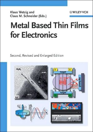
Metal Based Thin Films for Electronics
This up-to-date handbook covers the main topics of preparation, characterization and properties of complex metal-based layer systems. The authors — an outstanding group of researchers — discuss advanced methods for structure, chemical and electronic state characterization with reference to the properties of thin functional layers.\ This second edition has been completely revised and updated to reflect the rapid progress taking place in the field, including, for example, investigations of the...
Search in google:
This up-to-date handbook covers the main topics of preparation, characterization and properties of complex metal-based layer systems. The authors—an outstanding group of researchers—discuss advanced methods for structure, chemical and electronic state characterization with reference to the properties of thin functional layers, such as metallization and barrier layers for microelectronics, magnetoresistive layers for GMR and TMR, sensor and resistance layers. As such, the book addresses materials specialists in industry, especially in microelectronics, as well as scientists, and can also be recommended for advanced studies in materials science, analytics, surface and solid state science.
\ Metal Based Thin Films for Electronics\ \ \ \ John Wiley & Sons\ \ \ \ Copyright © 2003\ \ Klaus Wetzig, Claus M. Schneider\ All right reserved.\ \ \ ISBN: 3-527-40365-5\ \ \ \ Introduction\ \ \ Prologue\ Electronic devices have found widespread use in our everyday lives. The applications cover\ many areas such as consumer electronics, information technology, engineering, automotive\ application, transportation, medical diagnostics and treatments, etc. The construction of these\ devices and their building blocks involves elaborate fabrication processes which are based on\ a thorough understanding of materials science and solid state physics. The device functionality\ may involve conventional microelectronic, acoustoelectronic, optoelectronic, or future\ spinelectronic elements, or a combination of these (Figure 1.1). The functionality is achieved\ by a carefully engineered and complex combination of metallic, semiconducting, and insulating\ layers. These layers are often micro- and nanostructured by sophisticated lithography\ techniques in order to achieve the desired properties. Sometimes, as in the case of microprocessors,\ the structuring involves several levels. The individual feature sizes created by the\ structuring processes may be as small as 100 nm and are expected to become even smaller in\ the future in leading edge applications.\ [Figure 1.1 Omitted]\ The fabrication of these electronic devices requiresa very good control of the materials\ properties. This concerns not only the physical material parameters, but also the film structure\ and morphology. The latter are largely determined by the details of the deposition process\ and postgrowth processing procedures. In addition, the interfaces between different materials\ and material classes are also becoming of crucial importance. In this situation, a wide\ variety of analysis tools must be used to ensure a reliable process control and - if necessary - a\ precise failure analysis. These tools include not only different real space (microscopy) and\ reciprocal space (diffraction) techniques, but also spectroscopic techniques, electrical transport\ measurements, stress and strain analyses, migration investigations, etc.\ Novel device technologies are often closely linked to the use of new materials or material\ classes. One recent example is the replacement of the conventional Al interconnects in microprocessors\ by Cu ones. This step not only involves new fabrication procedures, such as\ the "damascene" technique, but also requires new barrier layers to avoid the mixing of Cu\ and Si. Another example is the emerging technology of magneto- or spinelectronics. In its\ present state it employs complex magnetic units composed of metal or metal/insulator layer\ stacks. In addition to the electrical properties, the layers must also provide a distinct magnetic\ functionality. Since all of the classical ferromagnets Fe, Co, Ni and many antiferromagnets\ used in magnetoelectronics are metals, this adds another and very exciting facet to\ the application of metal-based films in electronics.\ From the above considerations follows quite clearly that metal-based thin films play a\ central role in the different steps of the fabrication and for the specific functionality of electronic\ devices. The most evident use concerns conducting lines and interconnects. Less obvious\ is their employment as barrier layers against interdiffusion and segregation. Also very\ important are metallization layers, for example, in acoustoelectronic devices. In chemically\ complex systems, the physical properties can be conveniently changed by the chemical composition.\ This is particularly true for the conductivity and is exploited in silicides for thermoelectric\ applications. Metal-based films are also very important for X-ray optical techniques\ used to fabricate (X-ray lithography) and analyze (X-ray diffraction and spectroscopy)\ electronic device structures.\ Since metal-based films have such a widespread use in the different areas of microelectronics,\ knowledge of the respective properties and phenomena is distributed over various\ fields of physics and materials science. As a consequence, one usually has to consult many\ different sources in order to get the desired piece of information or a broader overview of a\ specific issue. Considering the importance of metal-based films in the field of electronics it is\ thus justified to describe and discuss these systems, the associated effects and phenomena,\ and their applications in one place.\ \ Organization, Aim and Content of This Book\ The main purpose of this book is two-fold. On the one hand, it is meant to serve as a compendium\ for metal-based thin film systems and their usage in electronics technology. As\ such, it addresses both the scientist and the research engineer. On the other hand, the book\ also includes a more tutorial part which is intended to bridge the gap between fundamental\ phenomena and their technological applications. It may therefore also serve as a textbook for\ advanced students in solid state physics, materials science, and electronics engineering.\ The book is organized into several chapters covering the range from principal aspects and\ phenomena over contemporary challenges in materials science to actual device concepts and\ applications. We thereby mainly concentrate on the relevant fields of interconnects, acoustoelectronics,\ thermoelectrics, magnetoelectronics, and X-ray optics.\ In Chapter 2 we review the various fundamental aspects of metal and metal-based films\ with respect to the individual fields and applications addressed in this book. This chapter is\ mainly intended to convey background information for the advanced student in a more tutorial\ form. It forms a basis for the discussion of the future challenges and the device-related\ topics in the subsequent chapters. The first section is devoted to a key aspect in microelectronics,\ namely the means to transfer and distribute information and power in a microelectronic\ device, for example, in a microprocessor. This is achieved by means of metallic interconnects\ which are usually arranged in very complicated and delicate three-dimensional\ networks. The contribution discusses both Al and Cu-based technologies for interconnects\ and highlights the specific implications and problems associated with each technology. A\ somewhat less familiar, though not less eminent area of microelectronics is acoustoelectronics.\ Acoustoelectronic devices are based on the exploitation of phenomena involving the\ generation, transport, and filtering of surface acoustic waves. Their functionality is largely\ determined by the interaction between a piezoelectric substrate and a metallic film serving as\ an electrode. Surface acoustic wave devices play a strategic role in telecommunication and\ other high frequency applications. A rather novel facet of microelectronics is called magnetoelectronics\ or "spintronics" which is the topic of the third section of Chapter 2. Spintronics\ is still an emerging technology which is based on the transport of spins and charges, rather\ than just charges. It thus combines magnetic functionalities and materials with established\ microelectronics concepts. Current spintronics applications concern read heads in hard disk\ drives, magnetocouplers, or nonvolatile magnetic random access memories (MRAM). In the\ long run, reprogrammable magnetic logic circuits or active magnetoelectronic devices, such\ as a spin transistor, may be expected. The section reviews the fundamental aspects of spindependent\ transport and magnetic coupling phenomena in thin films and layer stacks. It also\ discusses the basic thin film arrangements and their specific properties with respect to a\ particular device functionality. Thermoelectricity exploits the conversion of thermal energy\ into electrical energy and vice versa for power generators, cooling devices, and temperature\ or radiation sensors. The particular relevance of thermoelectrical systems for microelectronics\ arises - among other reasons - from the increasing need for efficient thermal and power\ management of chip devices. The implementation of Peltier elements in the chip architecture\ can provide on-chip cooling facilities. The recovery of excess heat and its conversion into\ electrical energy may help to reduce the overall power consumption and represents a step\ towards future self-sufficient systems. The different material systems and thermoelectric\ concepts which are currently under consideration are treated in the fourth section. Particular\ emphasis is put on the role of the various materials properties with respect to the thermoelectrical\ efficiency parameters and figure of merit. The final section of the chapter deals with\ the role of metallic layers and multilayer systems for X-ray optics. The connection of X-ray\ optics to microelectronics comes from the progress in optical lithography techniques which\ aim at feature sizes well below 100 nm. Because of the smaller wavelengths, the novel lithography\ approaches can no longer be based on transmission optics, but have to use reflective\ optics instead. Metal thin film systems are therefore needed to realize the appropriate\ optical elements (mirrors, gratings, etc.). The section discusses the fundamental aspects of X-ray\ optics with respect to thin film systems based on reflection and diffraction.\ Chapter 3 is devoted to the deposition techniques used to prepare thin film systems and to\ the main analytical approaches employed to study their behavior. The analysis involves microscopy,\ spectroscopy, or diffraction techniques and gives access to different properties,\ such as the film morphology, chemical composition, crystallographic and electronic structure.\ Deposition techniques for thin metallic films exist in a wide variety and are described in\ Chapter 3.1. Today vacuum based physical and also chemical deposition techniques play the\ dominant role in the preparation of thin metallic films, but non-vacuum based deposition\ methods such as electroplating or the modified CVD technique ALD (atomic layer deposition)\ are also of growing interest and will therefore be discussed in this book. Both transmission\ electron microscopy (TEM) and electron diffraction are strong techniques for studying\ micro- and nanostructures in metal based thin films. Furthermore, with enhancement of an\ analytical TEM by spectroscopic attachments for such as energy dispersive X-ray spectroscopy\ (EDXS) and electron energy-loss spectroscopy (EELS) it is also possible to receive\ chemical information (element distribution and chemical binding) in the nanometer range of\ thin films. A powerful method for the immediate study of electrical thin film properties is in\ situ scanning electron microscopy (SEM). In situ SEM methods allow the investigation of\ potential contrast, ferroelectric domains, electron beam induced current (EBIC) and processes\ of electro- or acoustomigration respectively. X-ray scattering techniques are discussed\ as a widely-used tool for structural information on thin films. Both the possibilities and limitations\ of angle diffraction, reflectometry, soft X-rays and magnetic scattering are discussed.\ Spectroscopic techniques allow the element distribution and depth profile analysis of thin\ films. They can be carried out by electrons, X-rays or ions and are frequently used in connection\ with imaging techniques such as scanning or transmission electron microscopy. In contrast\ to bulk materials, thin films on substrates are usually under mechanical stress. Thus,\ stress measurement methods play an important role in the characterization of thin films for\ electronics. Different techniques such as the substrate curvature and the [sin.sup.2] [PSI] method are\ discussed under application aspects.\ As one of the core parts of this book Chapter 4 addresses current challenges in the investigation\ and application of metal-based thin films. These include the aspects of thermal stability,\ acousto- and electromigration, barrier and nucleation layers, functional electric and\ magnetic layers and mulilayers for X-ray optical purposes. These topics represent the forefront\ of the current research in materials science and solid state physics. Because of the continuing\ downscaling in the architecture of integrated circuits electromigration is a life- limiting\ process in metallization layers. The damage analysis is discussed both for Al and Cu\ interconnects. The introduction of copper as the conducting material for interconnects requires\ effective diffusion barriers since copper readily diffuses into silicon oxide and silicon.\ The optimization of barriers and new barrier/ seed concepts are therefore the focus of attention.\ Migration effects are also observed in surface acoustic waves (SAW) structures, as a\ result of diminishing structure dimensions (< 1 µm) and increasing electrical input power\ values (> 1 W) which cause very high power density levels and therefore high stress loading\ of metallization. Thus, new metallization concepts have to be discussed in detail. Spintronic\ applications of functional magnetic layers, such as for sensors and MRAMs, may be realized\ by thin film systems which may be grouped into multilayers, spin valves and tunnel junctions.\ These systems excel in a precisely defined functionality which is strongly influenced\ by temperature. Therefore the thermal stability plays a dominant role in both the manufacture\ and operation of functional magnetic layers, as will be demonstrated for magnetoresistive\ layer stacks. A further group of thin film based components with growing importance are\ multilayers for X-ray optical purposes, e.g. as reflectors for X-rays. Finally, the last part of\ Chapter 4 is focused on functional electric layers with well-defined electronic and electrical\ transport properties. Such thin film materials are used as resistance layers, thermoelectric\ sensors and generator devices. The optimization of the electrical and thermoelectric film\ parameters will be discussed in depth.\ The application of metal-based thin film systems in electronic and microelectronics-related\ devices is the focus of Chapter 5. The diversity of the devices treated in this chapter\ highlights the widespread application areas of metal film systems. The first section deals\ with interconnect technologies for memory and logic products. Of particular interest are the\ combination of Cu interconnects and low-k dielectrics. The subsequent section on surface\ acoustic wave devices gives examples of high frequency filters, resonators and delay lines.\ The device concepts range from relatively simple transversal bandpass filters to programmable\ phase shift keying filters. The magnetic and magnetoelectronic sensor devices are mainly\ related to automotive applications and thus emphasize one of the growing future markets for\ microelectronics products. There, magnetic sensors are employed to measure positions, angles,\ rotational speeds, or torques with the aim of improving fuel economy, vehicle and passenger\ safety, and driving comfort in the present and new generations of automobiles. Reducing\ the energy consumption and improving the energy efficiency is also the driving force\ in the development of thermoelectric sensors and transducers.\ \ Continues...\ \ \ \ \ \ \ Excerpted from Metal Based Thin Films for Electronics\ \ Copyright © 2003 by Klaus Wetzig, Claus M. Schneider.\ Excerpted by permission.\ All rights reserved. No part of this excerpt may be reproduced or reprinted without permission in writing from the publisher.\ Excerpts are provided by Dial-A-Book Inc. solely for the personal use of visitors to this web site.\ \ \
1Introduction12Thin film systems : basic aspects7Interconnects for microelectronics7Metallization structures in acoutoelectronics28Silicide layers for electronics48Complex layered systems for magnetoelectronics71Multilayer and single-surface reflectors for X-ray optics103Metallic layers for photovoltaics1223Thin film preparation and characterization techniques141Thin film preparation methods141Electron microscopy and diffraction160X-ray scattering techniques179Spectroscopic techniques197Stress measurement techniques2144Challenges for thin film systems characterization and optimization231Electromigration in metallization layers231Barrier and nucleation layers for interconnects248Acoustomigration in surface acoustic waves structures261Thermal stability of magnetoresistive layer stacks283Functional magnetic layers for sensors and MRAMs295Multilayers for X-ray optical purposes309Functional electric layers3235Devices349Device related aspects for Si-based electronics349SAW high frequency filters, resonators and delay lines353Sensor devices362X-ray optical systems373Thermoelectric sensors and transducers3836Outlook399
\ From the Publisher"...I can certainly agree with the final sentence of the book cover: A perfect introduction to the field-for professionals and students."\ Angewandte Chemie 2004 No. 11, Uwe Bornscheuer\ "Through its focus on practical aspects and its didactic approach, the book is designed especially for practitioners. It can be highly recommended to materials engineers, physicists or process engineers who work or plan to work in the still exciting field of micro electronics."\ Winfried Blau, European Society of Thin Films, Dresden\ \ \
