Microelectronic Circuits
Fresh, new problems in Microelectronics—FREE with text!\ Package our new problems supplement with Microelectronic Circuits, Sixth Edition, and get:\ * 300 new problems\ * Solutions available exclusively to instructors\ Order pack ISBN: 978-0-19-993150-7\ This market-leading textbook continues its standard of excellence and innovation built on the solid pedagogical foundation that instructors expect from Adel S. Sedra and Kenneth C. Smith. All material in the sixth edition of Microelectronic...
Search in google:
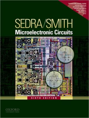
This market-leading textbook continues its standard of excellence and innovation built on the solid pedagogical foundation that instructors expect from Adel S. Sedra and Kenneth C. Smith. All material in the sixth edition of Microelectronic Circuits is thoroughly updated to reflect changes in technology—CMOS technology in particular. These technological changes have shaped the book's organization and topical coverage, making it the most current resource available for teaching tomorrow's engineers how to analyze and design electronic circuits. Features:* Streamlined organization. Short, modular chapters can be rearranged to suit any class organization. Topics that can be skipped on a first reading, while the student is grasping the basics, or that look ahead to advanced industrial applications, are clearly marked. * Digital Integrated Circuits covered in a new, separate section, to make it easier to teach Computer Engineering students.* Parallel Treatment of MOSFETs and BJTs. 90% of the market works with MOSFETs, so this vital topic is placed first in the textbook. The chapters on BJTs and MOSFETs are exactly parallel, so instructors can teach whichever one first that they prefer, and speed through the second topic by concentrating only on the differences between the two transistors.* Frequency response in a separate chapter. Frequency response is now condensed into a single chapter, rather than being integrated within other topics.New to this Edition:* Digital Circuits Early and Modular: New chapters in Part III: Digital Integrated Circuits make it easier to teach digital topics to computer engineers in a single-semester course.* New Chapter 13: CMOS Digital Logic Circuits lays the foundation for all digital material.* Frequency response in a separate chapter: Frequency response is now condensed into a single chapter (Ch. 9), rather than being integrated within other topics.* Streamlined and Signposted: Shorter, more modular chapters are easier to customize to any class. Visual cues and icons make the book easier to navigate. Explanations to the reader of why to read sections-and how multiple techniques might be used-are much more prominent. A new icon clearly marks topics that can be skipped on a first reading, while the student is grasping the basics, or that look ahead to advanced industrial applications.* Semiconductor primer in a separate chapter: For students who have not taken a prior course in Semiconductor Device Physics, Chapter 3 concisely covers the basics necessary to study Microelectronics. (Students who have had a device physics course will also find this a handy refresher.)* Lab-on-a-Disc: Offers complete simulations with activities, investigations, and directions to students for examples in the chapters and study problems from the ends of chapters. Simulated in MultisimTM and PSpice®. Also includes full student versions of MultisimTM and PSpice® so students can simulate their own activities and designs.* New Technical Coverage, including: a unique development of cascoding techniques (Ch 7); modern techniques for the design of BJT op amps (Ch 12); and deep submicron design and technology scaling (Ch 13). Please see the Preface for a complete list of the exciting new additions.Ancillaries:Instructor: [Note: Instructor's Resource CD is bound in to ISM-ISBN 9780195340303]* Instructor's Solutions Manual contains typed solutions to all in-text exercises and end-of-chapter problems.* PowerPoint Overheads on CD contain all of the figures with captions, plus summary tables, from the main text.Student:* In-text CD contains SPICE circuit simulation exercises and lessons, and a free student version of two SPICE simulators: OrCAD PSpice and Electronics Workbench Multisim.*'Companion website www.sedrasmith.org http://www.sedrasmith.org features SPICE models and links to industry and academic sites.
Brief Table of Contents Part I. Devices and Basic Circuits 1. Signals and Amplifiers 2. Operational Amplifiers 3. Semiconductors 4. Diodes 5. MOS Field-Effect Transistors (MOSFETs) 6. Bipolar Junction Transistors (BJTs) Part II. Integrated-Circuit Amplifiers 7. Building Blocks of Integrated-Circuit Amplifiers 8. Differential and Multistage Amplifiers 9. Frequency Response 10. Feedback 11. Output Stages and Power Amplifiers 12. Operational Amplifier Circuits Part III. Digital Integrated Circuits 13. CMOS Digital Logic Circuits 14. Advanced MOS and Bipolar Logic Circuits 15. Memory Circuits Part IV. Filters and Oscillators 16. Filters and Tuned Amplifiers 17. Signal Generators and Waveform-Shaping CircuitsFull Table of Contents Part I. Devices and Basic Circuits Chapter 1. Signals and Amplifiers Introduction 1.1 Signals 1.2 Frequency Spectrum of Signals 1.3 Analog and Digital Signals 1.4 Amplifiers 1.4.1 Signal Amplification 1.4.2 Amplifier Circuit Symbol 1.4.3 Voltage Gain 1.4.4 Power Gain and Current Gain 1.4.5 Expressing Gain in Decibels 1.4.6 Amplifier Power Supplies 1.4.7 Amplifier Saturation 1.4.8 Symbol Convention 1.5 Circuit Models for Amplifiers 1.5.1 Voltage Amplifiers 1.5.2 Cascaded Amplifiers 1.5.3 Other Amplifier Types 1.5.4 Relationships Between the Four Amplifier Models 1.5.5 Determining Ri and Ro 1.5.6 Unilateral Models 1.6 Frequency Response of Amplifiers 1.6.1 Measuring the Amplifier Frequency Response 1.6.2 Amplifier Bandwidth 1.6.3 Evaluating the Frequency Response of Amplifiers 1.6.4 Single-Time-Constant Networks 1.6.5 Classification of Amplifiers Based on Frequency Response Summary Problems Chapter 2. Operational Amplifiers (Op Amps) Introduction 2.1 The Ideal Op Amp 2.1.1 The Op-Amp Terminals 2.1.2 Function and Characteristics of the Ideal Op Amp 2.1.3 Differential and Common-Mode Signals 2.2 The Inverting Configuration 2.2.1 The Closed-Loop Gain 2.2.2 Effect of the Finite Open-Loop Gain 2.2.3 Input and Output Resistances 2.2.4 An Important Application: The Weighted Summer 2.3 The Noninverting Configuration 2.3.1 The Closed-Loop Gain 2.3.2 Effect of the Finite Open-Loop Gain 2.3.3 Input and Output Resistances 2.3.4 The Voltage Follower 2.4 Difference Amplifiers 2.4.1 A Single Op-Amp Difference Amplifier 2.4.2 A Superior Circuit: The Instrumentation Amplifier2.5 Integrators and Differentiators 2.5.1 The Inverting Configuration with General Impedances 2.5.2 The Inverting Integrator 2.5.3 The Op-Amp Differentiator 2.6 DC Imperfections 2.6.1 Offset Voltage 2.6.2 Input Bias and Offset Currents 2.6.3 Effect of Vos and Ios on the Operation of the Inverting Integrator 2.7 Effect of Finite Open-Loop Gain and Bandwidth on Circuit Performance 2.7.1 Frequency Dependence of the Open-Loop Gain 2.7.2 Frequency Response of the Closed-Loop Amplifier 2.8 Large-Signal Operation of Op Amps 2.8.1 Output Voltage Saturation 2.8.2 Output Current Limits 2.8.3 Slew Rate 2.8.4 Full-Power Bandwidth Summary Problems Chapter 3. Semiconductors 3.1 Intrinsic Semiconductors 3.2 Doped Semiconductors 3.3 Current Flow in Semiconductors 3.3.1 Drift Current 3.3.2 Diffusion Current 3.3.3 Relationship Between D and ? 3.4 The pn Junction with Open-Circuit Terminals (Equilibrium) 3.4.1 Physical Structure 3.4.2 Operation with Open-Circuit Terminals 3.5 The pn Junction with Applied Voltage 3.5.1 Qualitative Description of Junction Operation 3.5.2 The Current-Voltage Relationship of the Junction 3.5.3 Reverse Breakdown 3.6 Capacitive Effects in the pn Junction 3.6.1 Depletion or Junction Capacitance 3.6.2 Diffusion Capacitance Summary Problems Chapter 4. Diodes 4.1 The Ideal Diode 4.1.1 Current-Voltage Characteristic 4.1.2 A Simple Application: The Rectifier 4.1.3 Another Application: Diode Logic Gates 4.2 Terminal Characteristics of Junction Diodes 4.2.1 The Forward-Bias Region 4.2.2 The Reverse-Bias Region 4.2.3 The Breakdown Region 4.3 Modelling the Diode Forward Characteristic 4.3.1 The Exponential Model 4.3.2 Graphical Analysis Using the Exponential Model 4.3.3 Iterative Analysis Using the Exponential Model 4.3.4 The Need for Rapid Analysis 4.3.5 The Constant-Voltage Drop Model 4.3.6 The Ideal-Diode Model 4.3.7 The Small-Signal Model 4.3.8 Use of the Diode Forward Drop in Voltage Regulation 4.4 Operation in the Reverse Breakdown Region-Zener Diodes 4.4.1 Specifying and Modeling the Zener Diode 4.4.2 Use of the Zener as a Shunt Regulator 4.4.3 Temperature Effects 4.4.4 A Final Remark 4.5 Rectifier Circuits 4.5.1 The Half-Wave Rectifier 4.5.2 The Full-Wave Rectifier 4.5.3 The Bridge Rectifier 4.5.4 The Rectifier with a Filter Capacitor-The Peak Rectifier 4.5.5 Precision Half-Wave Rectifier-The Super Diode 4.6 Limiting and Clamping Circuits 4.6.1 Limiter Circuits 4.6.2 The Clamped Capacitor or DC Restorer 4.6.3 The Voltage Doubler 4.7 Special Diode Types 4.7.1 The Schottky-Barrier Diode (SBD) 4.7.2 Varactors 4.7.3 Photodiodes 4.7.4 Light-Emitting Diodes (LEDs) Summary Problems Chapter 5. MOS Field-Effect Transistors (MOSFETs) 5.1 Device Structure and Physical Operation 5.1.1 Device Structure 5.1.2 Operation with Zero Gate Voltage 5.1.3 Creating a Channel for Current Flow 5.1.4 Applying a Small ?DS 5.1.5 Operation as ?DS is Increased 5.1.6 Operation for ?DS ? VOV 5.1.7 The p-Channel MOSFET 5.1.8 Complementary MOS or CMOS 5.1.9 Operating the MOS Transistor in the Subthreshold Region 5.2 Current-Voltage Characteristics 5.2.1 Circuit Symbol 5.2.2 The iD- ?DS Characteristics 5.2.3 The iD-nuGS Characteristic 5.2.4 Finite Output Resistance in Saturation 5.2.5 Characteristics of the p-Channel MOSFET 5.3 MOSFET Circuits at DC 5.4 Applying the MOSFET in Amplifier Design 5.4.1 Obtaining a Voltage Amplifier 5.4.2 The Voltage Transfer Characteristic (VTC) 5.4.3 Biasing the MOSFET to Obtain Linear Amplification 5.4.4 The Small-Signal Voltage Gain 5.4.5 Determining the VTC by Graphical Analysis 5.4.6 Locating the Bias Point Q 5.5 Small-Signal Operation and Models 5.5.1 The DC Bias Point 5.5.2 The Signal Current in the Drain Terminal 5.5.3 Voltage Gain 5.5.4 Separating the DC Analysis and the Signal Analysis 5.5.5 Small-Signal Equivalent Circuit Models 5.5.6 The Transconductance gm 5.5.7 The T Equivalent Circuit Model 5.5.8 Summary 5.6 Basic MOSFET Amplifier Configurations 5.6.1 The Three Basic Configurations 5.6.2 Characterizing Amplifiers 5.6.3 The Common-Source Configuration 5.6.4 The Common-Source Amplifier with a Source Resistance 5.6.5 The Common-Gate Amplifier 5.6.6 The Common-Drain Amplifier or Source Follower 5.6.7 Summary and Comparisons 5.7 Biasing in MOS Amplifier Circuits 5.7.1 Biasing by Fixing VGS 5.7.2 Biasing by Fixing VG and Connecting a Resistance in the Source 5.7.3 Biasing Using a Drain-to-Gate Feedback Resistance 5.7.4 Biasing Using a Constant-Current Source 5.7.5 A Final Remark 5.8 Discrete-Circuit MOS Amplifiers 5.8.1 The Basic Structure 5.8.2 The Common-Source (CS) Amplifier 5.8.3 The Common-Source Amplifier with a Source Resistance 5.8.4 The Common-Gate Amplifier 5.8.5 The Source Follower 5.8.6 The Amplifier Bandwidth 5.9 The Body Effect and Other Topics 5.9.1 The Role of the Substrate-The Body Effect 5.9.2 Modeling the Body Effect 5.9.3 Temperature Effects 5.9.4 Breakdown and Input Protection 5.9.5 Velocity Saturation 5.9.6 The Depletion-Type MOSFET Summary Problems Chapter 6. Bipolar Junction Transistors (BJTs) 6.1 Device Structure and Physical Operation 6.1.1 Simplified Structure and Modes of Operation 6.1.2 Operation of the npn Transistor in the Active Mode Current Flow The Collector Current The Base Current The Emitter Current Recapitulation and Equivalent-Circuit Models 6.1.3 Structure of Actual Transistors 6.1.4 Operation in the Saturation Mode 6.1.5 The pnp Transistor 6.2 Current-Voltage Characteristics 6.2.1 Circuit Symbols and Conventions The Constant n Collector-Base Reverse Current (ICBO) 6.2.2 Graphical Representation of Transistor Characteristics 6.2.3 Dependence of iC on the Collector Voltage-The Early Effect 6.2.4 An Alternative Form of the Common-Emitter Characteristics The Common-Emitter Current Gain ? The Saturation Voltage VCEsat and Saturation Resistance RCEsat 6.3 BJT Circuits at DC 6.4 Applying the BJT in Amplifier Design 6.4.1 Obtaining a Voltage Amplifier 6.4.2 The Voltage Transfer Characteristic (VTC) 6.4.3 Biasing the BJT to Obtain Linear Amplification 6.4.4 The Small-Signal Voltage Gain 6.4.5 Determining the VTC by Graphical Analysis 6.4.6 Locating the Bias Point Q 6.5 Small-Signal Operation and Models 6.5.1 The Collector Current and the Transconductance 6.5.2 The Base Current and the Input Resistance at the Base 6.5.3 The Emitter Current and the Input Resistance at the Emitter 6.5.4 Voltage Gain 6.5.5 Separating the Signal and the DC Quantities 6.5.6 The Hybrid-? Model 6.5.7 The T Model 6.5.8 Small-Signal Models of the pnp Transistor 6.5.9 Application of the Small-Signal Equivalent Circuits 6.5.10 Performing Small-Signal Analysis Directly on the Circuit Diagram 6.5.11 Augmenting the Small-Signal Model to Account for the Early Effect 6.5.12 Summary 6.6 Basic BJT Amplifier Configurations 6.6.1 The Three Basic Configurations 6.6.2 Characterizing Amplifiers 6.6.3 The Common-Emitter Amplifier Characteristic Parameters of the CE Amplifier Overall Voltage Gain Alternative Gain Expressions Performing the Analysis Directly on the Circuit 6.6.4 The Common-Emitter Amplifier with An Emitter Resistance 6.6.5 The Common-Base (CB) Amplifier 6.6.6 The Common-Collector Amplifier or Emitter Follower The Need for Voltage Buffers Characteristic Parameters of the Emitter Follower Overall Voltage Gain Thévenin Representation of the Emitter Follower Output 6.6.7 Summary and Comparisons 6.7 Biasing in BJT Amplifier Circuits 6.7.1 The Classical Discrete-Circuit Biasing Arrangement 6.7.2 A Two-Power-Supply Version of the Classical Bias Arrangement 6.7.3 Biasing Using a Collector-to-Base Feedback Resistor 6.7.4 Biasing Using a Constant-Current Source 6.8 Discrete-Circuit BJT Amplifier 6.8.1 The Basic Structure 6.8.2 The Common-Emitter Amplifier 6.8.3 The Common-Emitter Amplifier with an Emitter Resistance 6.8.4 The Common-Base Amplifier 6.8.5 The Emitter Follower 6.8.6 The Amplifier Frequency Response 6.9 Transistor Breakdown and Temperature Effects 6.9.1 Transistor Breakdown 6.9.2 Dependence of ? on IC and Temperature Summary Problems Part II. Integrated-Circuit Amplifiers Chapter 7. Building Blocks of Integrated-Circuit Amplifiers 7.1 IC Design Philosophy 7.2 The Basic Gain Cell 7.2.1 The CS and CE Amplifiers with Current-Source Loads 7.2.2 The Intrinsic Gain 7.2.3 Effect of the Output Resistance of the Current-Source Load 7.2.4 Increasing the Gain of the Basic Cell 7.3 The Cascode Amplifier 7.3.1 Cascoding 7.3.2 The MOS Cascode 7.3.3 Distribution of Voltage Gain in a Cascode Amplifier7.3.4 The Output Resistance of a Source-Degenerated CS Amplifier 7.3.5 Double Cascoding 7.3.6 The Folded Cascode 7.3.7 The BJT Cascode 7.3.8 The Output Resistance of an Emitter-Degenerated CE Amplifier 7.3.9 BiCMOS Cascodes 7.4 IC Biasing-Current Sources, Current Mirrors, and Current-Steering Circuits 7.4.1 The Basic MOSFET Current Source 7.4.2 MOS Current-Steering Circuits 7.4.3 BJT Circuits 7.5 Current-Mirror Circuits with Improved Performance 7.5.1 Cascode MOS Mirrors7.5.2 A Bipolar Mirror with Base-Current Compensation 7.5.3 The Wilson Current Mirror 7.5.4 The Wilson MOS Mirror 7.5.5 The Widlar Current Source 7.6 Some Useful Transistor Pairings 7.6.1 The CC-CE, CD-CS, and CD-CE Configurations 7.6.2 The Darlington Configuration 7.6.3 The CC-CB and CD-CG Configurations Summary Appendix 7.A: Comparison of the MOSFET and BJT 7.A.1 Typical Values of IC MOSFET Parameters 7.A.2 Typical Values of IC BJT Parameters 7.A.3 Comparison of Important Characteristics 7.A.4 Combining MOS and Bipolar Transistors: BiCMOS Circuits 7.A.5 Validity of the Square-Law MOSFET Model Problems Chapter 8. Differential and Multistage Amplifiers 8.1 The MOS Differential Pair 8.1.1 Operation with a Common-Mode Input Voltage 8.1.2 Operation with a Differential Input Voltage 8.1.3 Large-Signal Operation 8.2 Small-Signal Operation of the MOS Differential Pair 8.2.1 Differential Gain 8.2.2 The Differential Half-Circuit 8.2.3 The Differential Amplifier with Current-Source Loads 8.2.4 Cascode Differential Amplifier 8.2.5 Common-Mode Gain and Common-Mode Rejection Ratio (CMRR) 8.3 The BJT Differential Pair 8.3.1 Basic Operation 8.3.2 Input Common-Mode Range 8.3.3 Large-Signal Operation 8.3.4 Small-Signal Operation 8.3.5 Common-Mode Gain and CMRR 8.4 Other Nonideal Characteristics of the Differential Amplifier 8.4.1 Input Offset Voltage of the MOS Differential Amplifier 8.4.2 Input Offset Voltage of the Bipolar Differential Amplifier 8.4.3 Input Bias and Offset Currents of the Bipolar Differential Amplifier 8.4.4 A Concluding Remark 8.5 The Differential Amplifier with Active Load 8.5.1 Differential to Single-Ended Conversion 8.5.2 The Active-Loaded MOS Differential Pair 8.5.3 Differential Gain of the Active-Loaded MOS Pair 8.5.4 Common-Mode Gain and CMRR 8.5.5 The Bipolar Differential Pair with Active Load 8.6 Multistage Amplifiers 8.6.1 A Two-Stage CMOS Op Amp 8.6.2 A Bipolar Op Amp Summary Problems Chapter 9. Frequency Response 9.1 Low-Frequency Response of the CS and CE Amplifiers 9.1.1 The CS Amplifier 9.1.2 The CE Amplifier 9.2 Internal Capacitive Effects and the High-Frequency Model of the MOSFET and the BJT 9.2.1 The MOSFET 9.2.2 The BJT 9.3 High-Frequency Response of the CS and CE Amplifiers 9.3.1 The Common-Source Amplifier 9.3.2 The Common-Emitter Amplifier 9.4 Useful Tools for the Analysis of the High-Frequency Response of Amplifiers 9.4.1 The High-Frequency Gain Function 9.4.2 Determining the 3-dB Frequency fH 9.4.3 Using Open-Circuit Time Constants for the Approximate Determination of fH 9.4.4 Miller's Theorem 9.5 A Closer Look at the High-Frequency Response of the CS and CE Amplifiers 9.5.1 The Equivalent Circuit 9.5.2 Analysis Using Miller's Theorem 9.5.3 Analysis Using Open-Circuit Time Constants 9.5.4 Exact Analysis 9.5.5 Adapting the Formulas for the Case of the CE Amplifier9.5.6 The Situation when Rsig is Low 9.6 High-Frequency Response of the CG and Cascode Amplifiers 9.6.1 High-Frequency Response of the CG Amplifier 9.6.2 High-Frequency Response of the MOS Cascode Amplifier 9.6.3 High-Frequency Response of the Bipolar Cascode Amplifier 9.7 High-Frequency Response of the Source and Emitter Followers 9.7.1 The Source Follower 9.7.2 The Emitter Follower 9.8 High-Frequency Response of Differential Amplifiers 9.8.1 Analysis of the Resistively Loaded MOS Amplifier 9.8.2 Analysis of the Active-Loaded MOS Amplifier 9.9 Other Wideband Amplifier Configurations 9.9.1 Obtaining Wideband Amplification by Source and Emitter Degeneration 9.9.2 The CD-CS, CC-CE and CD-CE Configurations 9.9.3 The CC-CB and CD-CG Configurations 9.10 High-Frequency Response of Multistage Amplifiers 9.10.1 Frequency Response of the Two-Stage CMOS Op Amp 9.10.2 Frequency Response of the Bipolar Op Amp of Section 8.5.2.Summary Problems Chapter 10. Feedback 10.1 The General Feedback Structure 10.2 Some Properties of Negative Feedback 10.2.1 Gain Desensitivity 10.2.2 Bandwidth Extension 10.2.3 Noise Reduction 10.2.4 Reduction in Nonlinear Distortion 10.3 The Four Basic Feedback Topologies 10.3.1 Voltage Amplifiers 10.3.2 Current Amplifiers 10.3.3 Transconductance Amplifiers 10.3.4 Transresistance Amplifiers 10.3.5 A Concluding Remark 10.4 The Feedback Voltage-Amplifier (Series-Shunt) 10.4.1 The Ideal Case10.4.2 The Practical Case 10.4.3 Summary 10.5 The Feedback Transconductance-Amplifier (Series-Series) 10.5.1 The Ideal Case 10.5.2 The Practical Case 10.5.3 Summary 10.6 The Feedback Transresistance-Amplifier (Shunt-Shunt) 10.6.1 The Ideal Case 10.6.2 The Practical Case 10.6.3 Summary 10.7 The Feedback Current-Amplifier (Shunt-Series) 10.7.1 The Ideal Case 10.7.2 The Practical Case 10.8 Summary of the Feedback Analysis Method10.9 Determining the Loop Gain 10.9.1 An Alternative Approach for Finding A? 10.9.2 Equivalence of Circuits from a Feedback-Loop Point of View 10.10 The Stability Problem 10.10.1 The Transfer Function of the Feedback Amplifier 10.10.2 The Nyquist Plot 10.11 Effect of Feedback on the Amplifier Poles 10.11.1 Stability and Pole Location 10.11.2 Poles of the Feedback Amplifier 10.11.3 Amplifier with a Single-Pole Response 10.11.4 Amplifier with a Two-Pole Response10.11.5 Amplifier with Three or More Poles 10.12 Stability Study Using Bode Plots 10.12.1 Gain and Phase Margins 10.12.2 Effect of Phase Margin on Closed-Loop Response 10.12.3 An Alternative Approach for Investigating Stability 10.13 Frequency Compensation 10.13.1 Theory 10.13.2 Implementation 10.13.3 Miller Compensation and Pole Splitting Summary Problems Chapter 11. Output Stages and Power Amplifiers 11.1 Classification of Output Stages 11.2 Class A Output Stage11.2.1 Transfer Characteristic 11.2.2 Signal Waveforms 11.2.3 Power Dissipation 11.2.4 Power Conversion Efficiency 11.3 Class B Output Stage 11.3.1 Circuit Operation 11.3.2 Transfer Characteristic 11.3.3 Power-Conversion Efficiency 11.3.4 Power Dissipation 11.3.5 Reducing Crossover Distortion 11.3.6 Single-Supply Operation 11.4 Class AB Output Stage 11.4.1 Circuit Operation 11.4.2 Output Resistance 11.5 Biasing the Class AB Circuit 11.5.1 Biasing Using Codes11.5.2 Biasing Using the VBE Multiplier 11.6 CMOS Class AB Output Stages 11.6.1 The Classical Configuration 11.6.2 An Alternative Circuit Utilizing Common-Source Transistors 11.7 Power BJTs 11.7.1 Junction Temperature 11.7.2 Thermal Resistance 11.7.3 Power Dissipation versus Temperature 11.7.4 Transistor Case and Heat Sink 11.7.5 The BJT Safe Operating Area 11.7.6 Parameter Values of Power Transistors 11.8 Variations on the Class AB Configuration 11.8.1 Use of Input Emitter Followers 11.8.2 Use of Compound and Devices11.8.3 Short-Circuit Protection 11.8.4 Thermal Shutdown 11.9 IC Power Amplifiers 11.9.1 A Fixed-Gain IC Power Amplifier 11.9.2 Power Op Amps 11.9.3 The Bridge Amplifier 11.10 MOS Power Transistors 11.10.1 Structure of the Power MOSFET 11.10.2 Characteristics of Power MOSFETs 11.10.3 Temperature Effects 11.10.4 Comparison with BJTs 11.10.5 A Class AB Output Stage Utilizing Power MOSFETs Summary Problems Chapter 12. Operational Amplifier Circuits 12.1 The Two Stage CMOS Op Amp 12.1.1 The Circuit 12.1.2 Input Common-Mode Range and Output Swing 12.1.3 Voltage Gain 12.1.4 Common-Mode Rejection Ratio (CMRR) 12.1.5 Frequency Response 12.1.6 Slew Rate 12.1.7 Power-Supply Rejection Ratio (PSRR) 12.1.8 Design Tradeoffs 12.2 The Folded Cascode CMOS Op Amp 12.2.1 The Circuit 12.2.2 Input Common-Mode Range and Output Swing 12.2.3 Voltage Gain 12.2.4 Frequency Response 12.2.5 Slew Rate12.2.6 Increasing the Input Common-Mode Range: Rail-to-Rail Input Operation 12.2.7 Increasing the Output Voltage Range: The Wide-Swing Current Mirror 12.3 The 741 Op-Amp Circuit 12.3.1 Bias Circuit 12.3.2 Short-Circuit Protection Circuitry 12.3.3 The Input Stage 12.3.4 The Second Stage 12.3.5 The Output Stage 12.3.6 Device Parameters 12.4 DC Analysis of the 741 12.4.1 Reference Bias Current 12.4.2 Input-Stage Bias 12.4.3 Input Bias and Offset Currents 12.4.4 Input Offset Voltage 12.4.5 Input Common-Mode Range12.4.6 Second-Stage Bias 12.4.7 Output-Stage Bias 12.5 Small-Signal Analysis of the 741 12.5.1 The Input Stage 12.5.2 The Second Stage 12.5.3 The Output Stage 12.6 Gain Frequency Response, Slew Rage of the 741 12.6.1 Small-Signal Gain 12.6.2 Frequency Response 12.6.3 A Simplified Model 12.6.4 Slew Rate 12.6.5 Relationship Between ft and SR 12.7 Modern Techniques for the Design of BJT Op Amps 12.7.1 Special Performance Requirements 12.7.2 Bias Design 12.7.3 Design of Input Stage to Obtain Rail-to-Rail ?ICM 12.7.4 Common-Mode Feedback to Control the DC Voltage at the Output of the Input Stage 12.7.5 Output-Stage Design for Near Rail-to-Rail Output Swing Summary Problems Part III. Digital Integrated Circuits Chapter 13. CMOS Digital Logic Circuits 13.1 Digital Logic Inverters 13.1.1 Function of the Inverter 13.1.2 The Voltage Transfer Characteristic (VTC) 13.1.3 Noise Margins 13.1.4 The Ideal VTC 13.1.5 Inverter Implementation13.1.6 Power Dissipation 13.1.7 Propagation Delay 13.1.8 Power-Delay and Energy-Delay Products 13.1.9 Silicon Area 13.1.10 Digital IC Technologies and Logic-Circuit Families 13.1.11 Styles for Digital System Design 13.1.12 Design Abstraction and Computer Aids 13.2 The CMOS Inverter 13.2.1 Circuit Operation 13.2.2 The Voltage Transfer Characteristic 13.2.3 The Situation When QN and QP are Not Matched 13.3 Dynamic Operation of the CMOS Inverter 13.3.1 Determining the Propagation Delay 13.3.2 Determining the Equivalent Load Capacitance C 13.3.3 Inverter Sizing 13.3.4 Dynamic Power Dissipation 13.4 CMOS Logic-Gate Circuits 13.4.1 Basic Structure 13.4.2 The Two-Input NOR Gate 13.4.3 The Two-Input NAND Gate 13.4.4 A Complex Gate 13.4.5 Obtaining the PUN from the PDN and Vice Versa 13.4.6 The Exclusive-OR Function 13.4.7 Summary of the Synthesis Method 13.4.8 Transistor Sizing 13.4.9 Effects of Fan-In and Fan-Out on Propagation Delay13.5 Implications of Technology Scaling: Issues in Deep-Submicron Design 13.5.1 Scaling Implications 13.5.2 Velocity Saturation 13.5.3 Subthreshold Conduction 13.5.4 Wiring-The Interconnect Summary Problems Chapter 14. Advanced MOS and Bipolar Logic Circuits 14.1 Pseudo-NMOS Logic Circuits 14.1.1 The Pseudo-NMOS Inverter 14.1.2 Static Characteristics 14.1.3 Derivation of the VTC 14.1.4 Dynamic Operation 14.1.5 Design 14.1.6 Gate Circuits 14.1.7 Concluding Remarks14.2 Pass-Transistor Logic Circuits 14.2.1 An Essential Design Requirement 14.2.2 Operation with NMOS Transistors as Switches 14.2.3 Restoring the Value of VOH to VDD 14.2.4 The Use of CMOS Transmission Gates as Switches 14.2.5 Pass-Transistor Logic Circuit Examples 14.2.6 A Final Remark 14.3 Dynamic MOS Logic Circuits 14.3.1 The Basic Principle 14.3.2 Nonideal Effects 14.3.3 Domino CMOS Logic14.3.4 Concluding Remarks 14.4 Emitter-Coupled Logic (ECL) 14.4.1 The Basic Principle 14.4.2 ECL Families 14.4.3 The Basic Gate Circuit 14.4.4 Voltage Transfer Characteristics 14.4.5 Fan-Out 14.4.6 Speed of Operation and Signal Transmission 14.4.7 Power Dissipation 14.4.8 Thermal Effects 14.4.9 The Wired-OR Capability 14.4.10 Final Remarks 14.5 BiCMOS Digital Circuits 14.5.1 The BiCMOS Inverter 14.5.2 Dynamic Operation 14.5.3 BiCMOS Logic Gates Summary Problems Chapter 15. Memory Circuits 15.1 Latches and Flip-Flops 15.1.1 The Latch 15.1.2 The SR Flip-Flop 15.1.3 CMOS Implementation of SR Flip-Flops 15.1.4 A Simpler CMOS Implementation of the Clocked SR Flip-Flop 15.1.5 D Flip-Flop Circuits 15.2 Semiconductor Memories: Types and Architectures 15.2.1 Memory-Chip Organization 15.2.2 Memory-Chip Timing 15.3 Random-Access Memory (RAM) Cells 15.3.1 Static Memory (SRAM) Cell 15.3.2 Dynamic Memory (DRAM) Cell 15.4 Sense Amplifiers and Address Decoders 15.4.1 The Sense Amplifier 15.4.2 The Row-Address Decoder 15.4.3 The Column-Address Decoder 15.4.4 Pulse-Generation Circuits 15.5 Read-Only Memory (ROM) 15.5.1 A MOS ROM 15.5.2 Mask-Programmable ROMs 15.5.3 Programmable ROMs (PROMs and EPROMs) Summary Problems Part IV. Filters and Oscillators Chapter 16. Filters and Tuned Amplifiers 16.1 Filter Transmission, Types, and Specification 16.1.1 Filter Transmission 16.1.2 Filter Types16.1.3 Filter Specification 16.2 The Filter Transfer Function 16.3 Butterworth and Chebyshev Filters 16.3.1 The Butterworth Filter 16.3.2 The Chebyshev Filter 16.4 First-Order and Second-Order Filter Functions 16.4.1 First-Order Filters 16.4.2 Second-Order Filter Functions 16.5 The Second-Order LCR Resonator 16.5.1 The Resonator Natural Modes 16.5.2 Realization of Transmission Zeros 16.5.3 Realization of the Low-Pass Function 16.5.4 Realization of the High-Pass Function 16.5.5 Realization of the Bandpass Function 16.5.6 Realization of the Notch Functions 16.5.7 Realization of the All-Pass Function 16.6 Second-Order Active Filters Based on Inductor Replacement 16.6.1 The Antoniou Inductance-Simulation Circuit 16.6.2 The Op Amp-RC Resonator 16.6.3 Realization of the Various Filter Types 16.6.4 The All-Pass Circuit 16.7 Second-Order Active Filters Based on the Two-Integrator-Loop Topology 16.7.1 Derivation of the Two-Integrator-Loop Biquad 16.7.2 Circuit Implementation 16.7.3 An Alternative Two-Integrator-Loop Biquad Circuit 16.7.4 Final Remarks 16.8 Single-Amplifier Biquadratic Active Filters 16.8.1 Synthesis of the Feedback Loop 16.8.2 Injecting the Input Signal 16.8.3 Generation of Equivalent Feedback Loops 16.9 Sensitivity 16.9.1 A Concluding Remark 16.10 Switched-Capacitor Filters 16.10.1 The Basic Principle 16.10.2 Practical Circuits 16.10.3 A Final Remark 16.11 Tuned Amplifiers 16.11.1 The Basic Principle 16.11.2 Inductor Losses 16.11.3 Use of Transformers 16.11.4 Amplifiers with Multiple Tuned Circuits 16.11.5 The Cascode and the CC-CB Cascade 16.11.6 Synchronous Tuning 16.11.7 Stagger-tuning Summary Problems Chapter 17. Signal Generators and Waveform-Shaping Circuits 17.1 Basic Principles of Sinusoidal Oscillators 17.1.1 The Oscillator Feedback Loop 17.1.2 The Oscillation Criterion 17.1.3 Nonlinear Amplitude Control 17.1.4 A Popular Limiter Circuit for Amplitude Control 17.2 Op-Amp-RC Oscillator Circuits17.2.1 The Wien-Bridge Oscillator 17.2.2 The Phase-Shift Oscillator 17.2.3 The Quadrature Oscillator 17.2.4 The Active-Filter-Tuned Oscillator 17.2.5 A Final Remark 17.3 LC and Crystal Oscillators 17.3.1 LC-Tuned Oscillators 17.3.2 Crystal Oscillators 17.4 Bistable Multivibrators 17.4.1 The Feedback Loop 17.4.2 Transfer Characteristics of the Bistable Circuit 17.4.3 Triggering the Bistable Circuit 17.4.4 The Bistable Circuit as a Memory Element 17.4.5 A Bistable Circuit with Noninverting Transfer Characteristics 17.4.6 Application of the Bistable Circuit as a Comparator 17.4.7 Making the Output Levels More Precise 17.5 Generation of Square and Triangular Waveforms Using Astable Multivibrators 17.5.1 Operation of the Astable Multivibrator 17.5.2 Generation of Triangular Waveforms 17.6 Generation of a Standardized Pulse-The Monostable Multivibrator 17.7 Integrated-Circuit Timers17.7.1 The 555 Circuit 17.7.2 Implementing a Monostable Multivibrator Using the 555 IC 17.7.3 An Astable Multivibrator Using the 555 IC 17.8 Nonlinear Waveform-Shaping Circuits 17.8.1 The Breakpoint Method 17.8.2 The Nonlinear-Amplification Method 17.9 Precision Rectifier Circuits 17.9.1 Precision Half-Wave Rectifier-The "Superdiode" 17.9.2 An Alternative Circuit 17.9.3 An Application: Measuring AC Voltages 17.9.4 Precision Full-Wave Rectifier 17.9.5 A Precision Bridge Rectifier for Instrumentation Applications 17.9.6 Precision Peak Rectifiers 17.9.7 A Buffered Precision Peak Detector 17.9.8 A Precision Clamping Circuit Summary Problems
\ BooknewsRevised and updated text for the core courses in electronic circuits taught to majors in electrical and computer engineering stresses development of the ability to analyze and design electronic circuits, both analog and digital, discrete and integrated. While the application of integrated circuits is covered, emphasis is placed on transistor circuit design. The prerequisite is a first course in circuit analysis. Annotation c. Book News, Inc., Portland, OR (booknews.com)\ \
