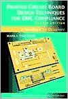
Printed Circuit Board Design Techniques for EMC Compliance
"Electromagnetic compatibility (EMC) is an engineering discipline often identified as "black magic." This belief exists because the fundamental mechanisms on how radio frequency (RF) energy is developed within a printed circuit board (PCB) is not well understood by practicing engineers. Rigorous mathematical analysis is not required to design a PCB. Using basic EMC theory and converting complex concepts into simple analogies helps engineers understand the mitigation process that deters EMC...
Search in google:
"Electromagnetic compatibility (EMC) is an engineering discipline often identified as "black magic." This belief exists because the fundamental mechanisms on how radio frequency (RF) energy is developed within a printed circuit board (PCB) is not well understood by practicing engineers. Rigorous mathematical analysis is not required to design a PCB. Using basic EMC theory and converting complex concepts into simple analogies helps engineers understand the mitigation process that deters EMC events from occurring. This user-friendly reference covers a broad spectrum of information never before published, and is as fluid and comprehensive as the first edition. The simplified approach to PCB design and layout is based on real-life experience, training, and knowledge. Printed Circuit Board Techniques for EMC Compliance, Second Edition will help prevent the emission or reception of unwanted RF energy generated by components and interconnects, thus achieving acceptable levels of EMC for electrical equipment. It prepares one for complying with stringent domestic and international regulatory requirements. Also, it teaches how to solve complex problems with a minimal amount of theory and math. Essential topics discussed include: * Introduction to EMC * Interconnects and I/O * PCB basics * Electrostatic discharge protection * Bypassing and decoupling * Backplanes-Ribbon Cables-Daughter Cards * Clock Circuits-Trace Routing-Terminations * Miscellaneous design techniques This rules-driven book-formatted for quick access and cross-reference-is ideal for electrical and EMC engineers, consultants, technicians, and PCB designers regardless ofexperience or educational background." Sponsored by: IEEE Electromagnetic Compatibility Society Booknews Presents a simplified approach to printed circuit board (PCB) design and layout, focusing on complying with domestic and international regulatory requirements. Coverage encompasses PCB basics, bypassing and decoupling, clock circuits, interconnects and I/O, electrostatic discharge protection, backplanes, ribbon cables, daughter cards, and design techniques. Appendices offer a summary of design techniques, and international EMC requirements. Theory and math are kept to a minimum to highlight practical techniques. Montrose is a senior member of the Institute of Electrical and Electronics Engineers. Annotation c. Book News, Inc., Portland, OR (booknews.com)
Printed Circuit Board Design Techniques for EMC Compliance\ A Handbook for Designers \ \ By Mark I. Montrose \ John Wiley & Sons\ ISBN: 0-7803-5376-5 \ \ \ Chapter One\ Introduction\ 1.1 FUNDAMENTAL DEFINITIONS\ The following basic terms are used throughout this book.\ Containment. A process whereby RF energy is prevented from exiting an enclosure, generally by shielding a product within a metal enclosure (Faraday cage or Gaussian structure) or by using a plastic housing with an RF conductive coating. Reciprocally, we can also speak of containment as preventing RF energy from entering the enclosure.\ Electromagnetic compatibility (EMC). The capability of electrical and electronic systems, equipment, and devices to operate in their intended electromagnetic environment within a defined margin of safety, and at design levels or performance, without suffering or causing unacceptable degradation as a result of electromagnetic interference (ANSI C64.14-1992).\ Electromagnetic interference (EMI). The lack of EMC, since the essence of interference is the lack of compatibility. EMI is the process by which disruptive electromagnetic energy is transmitted from one electronic device to another via radiated or conducted paths (or both). In common usage, the term refers particularly to RF signals. EMI can occur in the frequency range commonly identified as "anything greater than DC to daylight."\ Radio Frequency (RF). A frequency range containing coherent electromagnetic radiation of energy useful for communication purposes-roughly the range from 10 kHz to 100 GHz. This energy may be transmitted as a byproduct of an electronic device's operation. RF is transmitted through two basic modes:\ Radiated emissions. The component of RF energy that is transmitted through a medium as an electromagnetic field. RF energy is usually transmitted through free space; however, other modes of field transmission may occur.\ Conducted emissions. The component of RF energy that is transmitted through a medium as a propagating wave, generally through a wire or interconnect cables.\ Line Conducted Interference (LCI). Refers to RF energy in a power cord or AC mains input cable. Conducted signals do not propagate as fields but may propagate as conducted waves.\ Immunity. A relative measure of a device or a system's ability to withstand EMI exposure while maintaining a predefined performance level.\ Electrostatic discharge (ESD). A transfer of electric charge between bodies of different electrostatic potential in proximity to each other or through direct contact. This definition is observed as a high-voltage pulse that may cause damage or loss of functionality to susceptible devices. Although lightning differs in magnitude as a high-voltage pulse, the term ESD is generally applied to events of lesser amperage and more specifically to events triggered by human beings.\ Radiated immunity. A product's relative ability to withstand electromagnetic energy that arrives via free-space propagation.\ Conducted immunity. A product's relative ability to withstand electromagnetic energy that penetrates it through external cables, power cords, I/O interconnects, or chassis. EMI may also couple to a chassis, if interconnects are improperly implemented. Susceptibility. A relative measure of a device, or a system's propensity to be disrupted or damaged by EMI exposure to an incident field or signal. It is the lack of immunity.\ Suppression. The process of reducing or eliminating RF energy that exists without relying on a secondary method, such as a metal housing or chassis. Suppression may include shielding and filtering as well.\ 1.2 ELEMENTS OF THE ELECTROMAGNETIC ENVIRONMENT\ When an EMI problem occurs, the engineer needs to approach the situation logically. A simple EMI model has three elements:\ 1. There must be a source of energy.\ 2. There must be a receptor that is upset by this energy when the intensity of the electromagnetic interference is above a tolerable limit.\ 3. There must be a coupling path between the source and receptor for the unwanted energy transfer.\ For interference to exist, all three elements have to be present. If one of the three elements is removed, there can be no interference. It therefore becomes the engineer's task to determine which is the easiest element to remove. Generally, designing a PCB that eliminates most sources of RF interference is the most cost-effective approach (called suppression). The source of interference is the active element producing the original waveform. The PCB must be designed to keep the energy developed to only those sections of the assembly that require this energy. The second and third elements tend to be addressed with containment techniques. Figure 1.1 illustrates the relationship between these three elements and presents a list of items associated with each element.\ With respect to PCBs, observe the following:\ Noise sources are frequency generation circuits, component radiation within a plastic package, incorrect trace routing, ground bounce from digital logic, and commonmode currents developed within an assembly.\ The propagation path is the medium that carries the RF energy, such as free space or interconnects (common impedance coupling).\ Receptors are devices that easily accept interference from I/O cables, or by radiated means, transferring this harmful energy to circuits and devices susceptible to disruption.\ On the surface, a product must be designed for two levels of performance: one to minimize RF energy exiting an enclosure (emissions), and the other to minimize the amount of RF energy entering (susceptibility or immunity). Both emissions and immunity are transmitted by radiated or conductive means. This relationship is shown in Fig. 1.2. Also, it must be considered that a product must be compatible within itself, i.e., emitting levels must not compromise the performance of sensitive segments within the product.\ When dealing with emissions, a general rule-of-thumb is\ The higher the frequency, the greater the efficiency of a radiated coupling path; the lower the frequency, the greater the efficiency that a conducted coupling path will cause EMI. The extent of coupling depends on the frequency of the circuit and edge rate transition of digital components switching logic states and transfer mechanism.\ 1.3 NATURE OF INTERFERENCE\ EMC is grouped into two categories: internal and external. The internal category is the result of signal degradation along a transmission path, including parasitic coupling between circuits in addition to field coupling between internal subassemblies, such as a power supply to a disk drive. Stated more specifically, the problems are signal losses and reflections along the path, along with crosstalk between adjacent signal traces.\ External problems are divided into emissions and immunity. Emissions derive primarily from harmonics of clocks or other periodic signals. Remedies concentrate on containing the periodic signal to as small an area as possible, blocking parasitic coupling paths to the outside world.\ Susceptibility to external influences, such as ESD or radio frequency interference, is related initially to propagated fields that couple into I/O lines, which then transfer to the inside of the unit, and secondarily to case shielding. The principal recipients are high-speed transmission lines and sensitive adjacent traces, particularly those terminated with edge-triggered components.\ There are five major considerations when performing EMC analysis on a product or design.\ 1. Frequency. Where in the frequency spectrum is the problem observed?\ 2. Amplitude. How strong is the source energy level, and how great is its potential to cause harmful interference?\ 3. Time. Is the problem continuous (periodic signals), or does it exist only during certain cycles of operation (e.g., disk drive write operation or network burst transmission)?\ 4. Impedance. What is the impedance of both the source and receptor units, and the impedance of the transfer mechanism between the two?\ 5. Dimensions. What are the physical dimensions of the emitting device that cause emissions to occur? RF currents will produce electromagnetic fields that will exit an enclosure through chassis leaks that equal significant fractions of a wavelength or significant fractions of a "rise-time distance." Trace lengths on a PCB have a direct relationship as transmission paths for RF currents.\ Whenever an EMI problem is approached, it is helpful to review this list based on product application. Understanding these five items will clear up much of the mystery of how EMI exists within a PCB. Applying these five considerations teaches us that design techniques make sense in certain contexts but not in others. For example, single-point grounding is excellent when applied to low-frequency applications, but it is completely inappropriate for radio frequency signals, which is where most of the EMI problems occur. Many engineers blindly apply single-point grounding for all product designs, without realizing that additional and more complex problems are created using this grounding methodology.\ When designing a PCB, we are concerned with current flow within the assembly. Current is preferable to voltage for a simple reason: current always travels around a closed-loop circuit following one or more paths. It is to our advantage to direct or steer this current in the manner that is desired for proper system operation. To control the path that the current flows, we must provide a low-impedance, RF return path back to the source of the energy. We must also divert interference current away from the load or victim circuit. For those applications that require a high-impedance path from source to the load, consider all possible paths through which the return current may travel.\ 1.4 REGULATORY REQUIREMENTS-NORTH AMERICA\ Electrical and electronic products generate RF energy. Electromagnetic emission levels are set by rules and regulations mandated by domestic and international governments or agencies. In the United States, the Federal Communications Commission (FCC) regulates the use of radio and wire communications. The FCC is an independent government agency, responsible for ensuring interstate and international communication by radio, television, satellite, and cable.\ In Canada, Industry Canada (IC) is the agency responsible for regulating radio and wire communication. Industry Canada performs a function similar to that of the Federal Communications Commission. Harmonized test requirements and standards for North America exist between both the FCC and IC.\ The FCC regulates electronic products by specifying technical standards and operational requirements through the Code of the Federal Register (CFR), Title 47. The sections within 47CFR that are most applicable to products discussed herein are Parts 2, 15, 18, and 68. These regulations, developed over many years, are based on complaints filed with the Commission. The most prominent FCC Parts are summarized in the following list. In Canada, the specification equivalent to 47CFR, Part 15, is SOR 88/475.\ 1. Part 2 is an administrative section that details aspects of how to comply with 47CFR. Included are allocated frequency bands, radio treaty matters, and general rules and regulations. The rules and regulations include registration requirements, authorization procedures, definitions, and various processes to ensure that the federal code is properly administered.\ 2. Part 15 regulates products that generate unlicensed radio frequency energy, both intentional and non-intentional. Information Technology Equipment (ITE) falls within Part 15.\ 3. Part 18 regulates Industrial, Scientific, and Medical (ISM) equipment. These devices use radio waves for proper operation.\ 4. Part 68 regulates electronic equipment connected to a telephone network. This part provides a uniform standard for protecting the telephone network from harm caused by connection of terminal equipment.\ The FCC defines a digital device as\ An unintentional radiator (device or system) that generates and uses timing signal or pulses at a rate in excess of 9,000pulses (cycles) per second and uses digital techniques; inclusive of telephone equipment that uses digital techniques or any device or system that generates and uses radio frequency energy for the purpose of performing data processing functions, such as electronic computations, operations, transformation, recording, filing, sorting, storage, retrieval or transfer.\ Digital computing products are classified into two categories: Class A and B. The FCC and IC use the same definitions.\ Class A: A digital device that is marketed for use in a commercial, industrial, or business environment, exclusive of a device which is marketed for use by the general public or is intended to be used in the home.\ Class B: A digital device that is marketed for use in a residential environment, notwithstanding its use in a commercial, industrial, or business environment. Examples of such devices include, but are not limited to, personal computers, calculators, and similar electronic devices that are marketed for use by the general public.\ If a product contains digital circuitry and has a clock frequency greater than 9 kHz, it is defined as a digital device and is subject to the rules and regulations of the FCC and IC. Electromagnetic Interference (EMI) may occur as a result of both digital and analog circuits. These products are subject to domestic and international regulatory requirements.\ 1.5 REGULATORY REQUIREMENTS-WORLDWIDE\ Test requirements, standards, and procedures have been harmonized on a worldwide basis. The principles discussed herein will allow regulatory compliance to be achieved with minimal development cost and shorter design cycles. The harmonization process is based on the work of expert technical committees reporting to the International Electrotechnical Commission (IEC).\ The IEC works closely with the International Standards Organization (ISO), which is chartered by the United Nations. Many countries throughout the world are members. The IEC oversees the work of technical committees working on a particular product sector. The IEC's objectives are to "promote international co-operation on all questions of standardization ... achieved by issuing publications including recommendations in the form of international standards."\ Two IEC technical committees work on EMC standards. The first is TC77, Electromagnetic compatibility between equipment including networks. The second committee is International Special Committee on Radio Interference (Comite International Special des Perturbations Radioelectriques or CISPR). CISPR publications deal primarily with limits and measurements of the radio interference characteristics of potentially disturbing sources or emissions. CISPR and IEC standards coexist to define most technical aspects related to EMC compliance.\ The IEC publications themselves have no legal requirements. National committees do not have to adopt them, although several countries outside of Europe have incorporated them into their national laws. The important aspect of IEC standards is that they have been adopted and harmonized as a European standard for all members of the European Union. Once published as a harmonized document, a legal requirement now exists.\ A separate organization, the Committee for European Electrotechnical Standardization (Comite Europeen de Normalisation Electrotechnique, or CENELEC), is responsible for developing European standards for electrical equipment. CENELEC received its charter from the Parliamentary Commission of the European Union and produces EMC standards for use with the EMC Directive, usually based on IEC and CISPR publications.\ For telecommunications equipment, the European Telecommunications Standards Institute, or ETSI, is the standards-making body. ETSI develops standards for telecommunications network equipment not supplied to the subscriber, in addition to radio communication equipment and broadcast transmitters.\ (Continues...)\ \ \ \ \ Excerpted from Printed Circuit Board Design Techniques for EMC Compliance by Mark I. Montrose Excerpted by permission.\ All rights reserved. No part of this excerpt may be reproduced or reprinted without permission in writing from the publisher.\ Excerpts are provided by Dial-A-Book Inc. solely for the personal use of visitors to this web site. \ \
Preface.Acknowledgments.List of Figures.List of Tables.Introduction.Printed Circuit Board Basics.Bypassing and Decoupling.Clock Circuits, Trace Routing, and Terminations.Interconnects and I/O.Electrostatic Discharge Protection.Backplanes, Ribbon Cables, and Daughter Cards.Additional Design Techniques.Appendix A: Summary of Design Techniques.Appendix B: International EMC Requirements.Appendix C: The Decibel.Appendix D: Conversion Tables.Bibliography and References.Index.About the Author.
\ BooknewsPresents a simplified approach to printed circuit board (PCB) design and layout, focusing on complying with domestic and international regulatory requirements. Coverage encompasses PCB basics, bypassing and decoupling, clock circuits, interconnects and I/O, electrostatic discharge protection, backplanes, ribbon cables, daughter cards, and design techniques. Appendices offer a summary of design techniques, and international EMC requirements. Theory and math are kept to a minimum to highlight practical techniques. Montrose is a senior member of the Institute of Electrical and Electronics Engineers. Annotation c. Book News, Inc., Portland, OR (booknews.com)\ \
